Baru 30 Pcb Routing Motif Minimalis, Skema Pcb
Poin pembahasan Baru 30 Pcb Routing Motif Minimalis, Skema Pcb adalah :
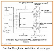
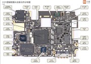
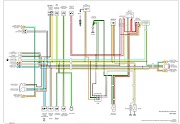
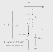
Baru 30 Pcb Routing Motif Minimalis, Skema Pcb. Berikut Penjelasan lengkap tentang fungsi komponen-komponen skema pcb dari yang aktif hingga pasif, prinsip cara kerjanya serta simbol yang wajib difahami. Perhatikan komponen skema pcb jenis resistor berikut yang dilengkapi dengan gambar. Simak ulasan terkait skema pcb dengan artikel Baru 30 Pcb Routing Motif Minimalis, Skema Pcb berikut ini

Watch routing PCB Layout with DDR3 High Speed Interfaces Sumber : www.youtube.com

professional router equipment Sumber : pcb-depanelizer.com

What s The Difference PCB Routing Then and Now Sumber : www.electronicdesign.com

Cnc Pcb Router Pcb Board Routing Machine ysvc 650 Buy Sumber : www.alibaba.com

PADS Webinar AutoRouter for High Speed PCB Routing Sumber : www.pads.com

pcb Routing USB2 signals Electrical Engineering Stack Sumber : electronics.stackexchange.com
1Select the Route tool on the left-hand side of your interface., 2Next, press Spacebar to cycle through the available routable layers. ..., 3Once your layer is selected, left-click on your first net to start your connection., 1Adopt DIY approach in making schematic. ..., 2Properly space the components. ..., 3Do not place traces at right angle. ..., 4Ensure same orientation while placing components. ..., 5Use different wiring directions between two consecutive layers. ..., 6Select the line width for facilitating easy current flow. ..., 7Creating ground plane.,

7 PCB Routing and Rules YouTube Sumber : www.youtube.com

Top 10 PCB Routing Tips for Beginners EAGLE Blog Sumber : www.autodesk.com

What s The Difference PCB Routing Then and Now Sumber : www.electronicdesign.com

What s The Difference PCB Routing Then and Now Sumber : www.electronicdesign.com

PCB Router Machine Automatic Hibex India Private Limited Sumber : www.indiamart.com

Top 10 PCB Routing Tips for Beginners EAGLE Blog Sumber : www.autodesk.com

One point three axis non CNC PCB routing jig YouTube Sumber : www.youtube.com

Milling PCBs with cheap Chinese desktop CNC router Off Sumber : forum.electricunicycle.org

Interactive PCB Routing and Placement Mentor Graphics Sumber : www.pads.com
1Select the Route tool on the left-hand side of your interface., 2Next, press Spacebar to cycle through the available routable layers. ..., 3Once your layer is selected, left-click on your first net to start your connection., 1Adopt DIY approach in making schematic. ..., 2Properly space the components. ..., 3Do not place traces at right angle. ..., 4Ensure same orientation while placing components. ..., 5Use different wiring directions between two consecutive layers. ..., 6Select the line width for facilitating easy current flow. ..., 7Creating ground plane.,
Baru 30 Pcb Routing Motif Minimalis, Skema Pcb. Berikut Penjelasan lengkap tentang fungsi komponen-komponen skema pcb dari yang aktif hingga pasif, prinsip cara kerjanya serta simbol yang wajib difahami. Perhatikan komponen skema pcb jenis resistor berikut yang dilengkapi dengan gambar. Simak ulasan terkait skema pcb dengan artikel Baru 30 Pcb Routing Motif Minimalis, Skema Pcb berikut ini
Watch routing PCB Layout with DDR3 High Speed Interfaces Sumber : www.youtube.com
High Speed PCB Routing Techniques to Reduce the Influence
PCB design programmes offer a huge amount of capability to enable the layout and routing to be achieved but in order to utilise these capabilities to the best effect a robust process must be used to ensure that all the requirements are met and the best PCB performance is obtained
professional router equipment Sumber : pcb-depanelizer.com
Routing Autorouting PCB Layout Basics 2 EAGLE Blog
PCB Routing Request Quote Micron Laser Technology s precision PCB routing or contouring services are provided for both rigid and flexible circuit board manufacturers Laser routing is ideal for close tolerance flexible circuits FPC before investing in expensive punch tooling e g small form fit devices or ZIF connectors Laser contouring is also a great
What s The Difference PCB Routing Then and Now Sumber : www.electronicdesign.com
DDR Routing Techniques in Your PCB Design Advanced PCB
EAGLE Academy How To Tips and Tricks PCB Layout Basics Part 2 How to Route or Autoroute Your PCB Design If component placement is a work of engineering art then routing can be understood as a puzzle just waiting to be solved
Cnc Pcb Router Pcb Board Routing Machine ysvc 650 Buy Sumber : www.alibaba.com
PCB Routing Topologies Demystified
16 08 2020 Sometimes routing a printed circuit board can feel the same way When first laying out a PCB design the tangled mess of nets going everywhere can seem like the same old battle of the shoe laces except that now there are 2 000 pairs of shoes to deal with
PADS Webinar AutoRouter for High Speed PCB Routing Sumber : www.pads.com
PCB Routing Micron Laser Technology
Detailed design rules in terms of layout routing and filter in high speed PCB design EMI design methods and some notices based on those methods in order to reduce the influence of EMI on the performance of PCB and to improve the reliability of PCB
pcb Routing USB2 signals Electrical Engineering Stack Sumber : electronics.stackexchange.com
PCB Routing Guidelines for Altium Designer
19 08 2020 1967 Shelby GT500 Barn Find and Appraisal That Buyer Uses To Pay Widow Price Revealed Duration 22 15 Jerry Heasley Recommended for you New
1Select the Route tool on the left-hand side of your interface., 2Next, press Spacebar to cycle through the available routable layers. ..., 3Once your layer is selected, left-click on your first net to start your connection., 1Adopt DIY approach in making schematic. ..., 2Properly space the components. ..., 3Do not place traces at right angle. ..., 4Ensure same orientation while placing components. ..., 5Use different wiring directions between two consecutive layers. ..., 6Select the line width for facilitating easy current flow. ..., 7Creating ground plane.,
7 PCB Routing and Rules YouTube Sumber : www.youtube.com
Top 10 PCB Routing Tips for Beginners EAGLE Blog
01 06 2020 PCB routing topologies are simply configurations for laying components and traces on a board In many ways a PCB can be thought of as a network data must flow from one point to another and it s important to optimize routing topology to ensure signal
Top 10 PCB Routing Tips for Beginners EAGLE Blog Sumber : www.autodesk.com
7 PCB Routing and Rules YouTube
What s The Difference PCB Routing Then and Now Sumber : www.electronicdesign.com
PCB Layout Routing Electronics Notes
Superior Routing Using Altium Designer as Your PCB Design Tools The routing on your PCB design is a critical part of the job but that doesn t mean that it has to be a nightmare for you to accomplish
What s The Difference PCB Routing Then and Now Sumber : www.electronicdesign.com
PCB Router Machine Automatic Hibex India Private Limited Sumber : www.indiamart.com
Top 10 PCB Routing Tips for Beginners EAGLE Blog Sumber : www.autodesk.com
One point three axis non CNC PCB routing jig YouTube Sumber : www.youtube.com
Milling PCBs with cheap Chinese desktop CNC router Off Sumber : forum.electricunicycle.org
Interactive PCB Routing and Placement Mentor Graphics Sumber : www.pads.com


0 Comments